

RAYPCB | Since 2005 🌍 🔌 Premium PCB Manufacturing ⚡ Reliable PCB Assembly (PCBA) 💡 Contract EMS Supplier ✨ Fast Turnkey Solutions | Global Shipping
shenzhen
Joined January 2017
- Tweets11.2K
- Following4.2K
- Followers7K
- Likes970



USB Communication Basics: PCB Layout & Routing Notes That Actually Matter 💡
USB is everywhere in embedded design.
But in practice, most USB issues aren't protocol problems — they're layout and routing problems.
Here's a quick refresher on USB basics + the PCB rules that separate working prototypes from field failures.
🔹 USB communication in simple terms
USB handles both data and power over the same cable.
Host (PC, hub) initiates all communication
Device (MCU, peripheral) responds
Data travels over a differential pair (D+/D−)
Common versions to know:
→ USB 2.0: 480 Mbps, still the workhorse
→ USB 3.x: higher speed, extra pairs
→ USB Type‑C: reversible, now mainstream
🔹 Key PCB layout guidelines
1️⃣ Component placement first
USB connector close to board edge
MCU close to connector → short data traces
ESD protection as close to connector as possible (limits ESD current from entering the PCB)
2️⃣ Routing rules for D+/D−
Route as a matched differential pair
Keep equal length, parallel, constant spacing
Target 90Ω differential impedance
Avoid sharp corners, stubs, and unnecessary detours
3️⃣ Ground reference & shielding
Solid ground plane under the USB pair
Add ground shielding if routed on outer layers
Never split the ground under USB signals — a clean return path is critical
4️⃣ Via usage
Minimize vias on D+/D− (each via adds impedance discontinuity)
If vias are unavoidable, keep them symmetric on both lines
🔹 Common mistakes that kill USB
❌ Routing USB next to switching power traces
❌ Long, winding D+/D− routes
❌ ESD protection placed far from connector
❌ Broken or noisy ground under the USB pair
Result: enumeration failures, unstable connections, or EMC headaches.
🔹 A DFM reality check
Poor impedance control → board‑to‑board variation
Excessive vias → lower yield at higher speeds
Clear stack‑up definition is required for consistent 90Ω differential impedance
"Good design is buildable design."
What's the strangest USB layout issue you've debugged? 👇
#PCBDesign #USB #HighSpeedDesign #SignalIntegrity #HardwareDesign #DFM

MOSFET Gate Resistor: Why It Matters & How to Choose It ⚡
When designing power electronics, it’s easy to focus solely on the MOSFET. But a tiny component between the driver and gate—the gate resistor (Rg)—deserves just as much attention.
Why? Because Rg directly impacts switching behavior, efficiency, and EMI.
🔹 What does the gate resistor do?
Placed between the driver output and MOSFET gate, Rg:
• Limits peak gate current
• Controls switching speed (dv/dt, di/dt)
• Reduces EMI and ringing
• Protects the driver IC
• Helps prevent parasitic turn-on
🔹 Gate current & driver power
Peak gate current ≈ Vdrive / (Rdriver + Rg)
Driver power ≈ ½ · Qg · Vdrive · fsw
Always ensure peak current stays within driver limits. And don’t overlook the gate charge curve and Miller plateau when selecting Rg.
🔹 Efficiency vs. EMI – the classic trade-off
• Large Rg → slower switching, higher loss, lower EMI
• Small Rg → faster switching, lower loss, higher EMI
The right value is almost always a conscious balance, not an extreme.
🔹 Practical tips
✅ Use separate turn-on (RGon) and turn-off (RGoff) resistors – a diode can create two paths. A good starting point: RGon ≈ 2 × RGoff
✅ Watch for gate loop inductance – fast di/dt can cause voltage spikes. Rg helps dampen oscillations.
✅ Beware of the Miller effect – drain voltage transitions can couple through Cgc and cause parasitic turn-on, especially in half-bridges.
🔹 Layout matters
• Place Rg as close as possible to the MOSFET gate
• Minimize gate loop area
• Keep gate traces short
• Use Kelvin source connections where feasible
Takeaway – The gate resistor is small in size but huge in influence. Choose it wisely, and pair it with good PCB layout for stable, efficient switching.
#PowerElectronics #MOSFET #HardwareDesign #EMI #PCBDesign #EngineeringTips


Choosing the right microcontroller can make or break your robotics, IoT, or AI project. 🎯
Performance, cost, and learning outcomes all hinge on this one decision. Yet many students and educators struggle to know where to start.
I’ve created a simple visual guide that breaks down the most widely used microcontrollers and their ideal use cases:
🔹 Arduino Uno – Best for beginners & foundational learning
🔹 ESP32 – Go-to for IoT, AI, and wireless communication
🔹 ESP8266 – Low-cost solution for basic Wi-Fi projects
🔹 Arduino Nano – Compact, great for small robotic systems
🔹 Raspberry Pi Pico – Fast, affordable, excellent for embedded learning
🔹 STM32 – Industrial and high-performance applications
🔹 ATtiny85 – Ultra low‑power, compact designs
🔹 Teensy – High‑speed, real‑time processing
Quick recommendations:
👉 Beginners → Arduino Uno or Nano
👉 IoT projects → ESP32
👉 Advanced robotics → STM32
👉 AI / voice systems → ESP32 or Raspberry Pi Pico
As a Robotics and STEM educator, I’ve seen how clear, early guidance builds students’ confidence and sparks innovation. That’s exactly why I put this poster together — to make complex concepts more accessible and help learners pick the right tool for the job.
What’s your go-to microcontroller for teaching or building? Let me know in the comments. 👇
#Robotics #IoT #ArtificialIntelligence #STEMeducation #Microcontrollers

🚀 Analog Layout Series – PNP Transistor Breakdown
Strong fundamentals = strong layouts.
Today, we’re diving into the PNP Bipolar Junction Transistor (BJT) — a key building block in many analog and mixed-signal layouts.
🔹 Structure: P–N–P layers
🔹 Current flow: Emitter → Collector
🔹 Turn-on condition: Emitter voltage > Base voltage
🔹 Majority carriers: Holes
🔹 Key relation: Iₑ = I𝒸 + Iᵦ
📌 Quick mnemonic:
PNP = Points I N (arrow points toward the base)
💡 Common applications:
• Amplifiers
• Switching circuits
• Current mirrors
• Analog signal processing
Whether you're just starting out or sharpening your analog skills, mastering devices like the PNP is what separates good layouts from great ones.
Let’s keep learning and growing together in the world of Analog Layout Design 🚀
Thank you all for your continued support 🙏
Special thanks to VLSI!
Feel free to add relevant hashtags like:
#AnalogLayout #VLSI #BJTs #Semiconductor #ChipDesign #EngineeringMindset

Inheriting a schematic and BOM with zero institutional knowledge is a humbling rite of passage in hardware development.
On the surface, everything looks fine:
✅ ERC/DRC passes
✅ BOM has part numbers
✅ All seems accounted for on paper
Then you start working with it.
❓ Why this op-amp instead of a rail-to-rail alternative?
❓ Why a 4.7k pull-up and not 10k?
❓ Why is there a DNP resistor here with no note explaining its purpose?
You dig through datasheets, trying to reverse-engineer decisions made years ago. Sometimes you find the answer. Often, you don’t.
The real cost hits when something changes—a part goes EOL, or a new revision touches an area you don’t fully understand. A simple update becomes a risk assessment, because you can’t tell what you’re allowed to change.
Good documentation isn’t just comments in a schematic. It’s capturing intent: why a part was chosen, what it compensates for, and what constraints existed at the time. A few sentences per non-obvious decision pays huge dividends for whoever picks up the design next—including future you, 18 months from now.
#HardwareEngineering #PCBDesign #Documentation #EngineeringLessons

A PCB’s thermal journey is about far more than hitting a peak temperature. It’s about how you control every stage along the way.
🌡️ The 4 critical stages of reflow:
Preheat (Ambient → ~120°C)
Gradual ramp prevents thermal shock and activates solvents.
Soak (120°C → 180°C)
Stabilizes temperature and activates flux for proper wetting.
Reflow (245°C → 260°C peak)
Solder melts, forming the actual electrical connection.
Cooling (↓ to ~75°C)
Controlled cooling (3–6°C/sec) determines joint strength and prevents tombstoning.
But here’s the reality:
Even with a perfect profile…
👉 Reflow cannot fix upstream issues.
It only exposes them:
• Inconsistent solder paste volume
• Component misalignment
• Printing defects
Why this matters:
→ Consistent process control = higher yield + fewer rework costs
→ Stronger, more reliable solder joints
→ Fewer field failures
→ Smoother, faster production throughput
Now over to you: which stage is the hardest to control in your process?
🔼 Preheat | 🌡 Soak | 🔥 Reflow | ❄️ Cooling
#PCB #SMT #Reflow #ElectronicsManufacturing #PCBA #Engineering #DFM #Manufacturing #HardwareDesign

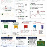
RC Snubber for 220VAC: Don’t Let the Wrong Capacitor Ruin Your Design ⚡
Switching AC loads (relays, triacs, motors)?
Voltage spikes are unavoidable — but you can control them with a properly designed RC snubber.
👇 Here’s what you need to know:
🔹 What is an RC snubber?
A resistor + capacitor in series, connected in parallel with the switching element or the inductive load.
🔹 Why use it?
✔️ Suppresses voltage spikes (transients)
✔️ Reduces arcing on relay contacts
✔️ Protects triacs & switches
✔️ Lowers EMI noise
🔹 Where to connect it?
• Across relay contacts
• Across triac (MT1–MT2)
• Across inductive load (motor, solenoid, pump)
🔹 Capacitor type — this is critical
✅ Recommended: Polypropylene film capacitor (Class X2)
→ Rated ≥ 275VAC
→ Designed for across-mains use
→ High pulse handling + self-healing
⚠️ Acceptable (with caution): Non-X2 polypropylene
→ Must be properly rated for AC & pulses
❌ Not suitable:
• Polyester (Mylar) — poor surge handling
• Ceramic — can crack under AC stress
• Electrolytic — polarized, unsafe on AC
🔹 Typical values (220VAC)
• Capacitor: 100nF (0.1µF) X2
• Resistor: 47Ω – 100Ω (≥ 0.5W)
🔹 Pro tips
✔️ Place snubber close to the switching element
✔️ Respect creepage & clearance
✔️ Voltage rating alone isn’t enough — type matters
🎯 Bottom line:
A snubber only works if you choose the right components.
👉 Stick with X2 polypropylene capacitors for safe, reliable designs.
#PCBDesign #Electronics #HardwareTips #EmbeddedSystems #PowerElectronics

CST vs ADS vs HFSS – Which RF simulation tool should you choose?
In RF design, your simulation tool isn't just software — it's your decision engine.
The right choice depends entirely on the problem you're solving.
Let's break it down:
🔹 ADS (Advanced Design System)
Best for circuit-level RF design
S-parameters, matching networks, harmonic balance
Fast simulations for RF chains (LNA, PA, mixers)
Ideal for system-level design & optimization
👉 Use ADS when your design starts at the schematic level.
🔹 HFSS
Best for 3D EM accuracy
High-precision electromagnetic simulation
Antennas, connectors, waveguides
Industry gold standard for accuracy
👉 Use HFSS when accuracy matters more than speed.
🔹 CST Studio Suite
Best for full-system EM + speed
Time-domain solver → faster broadband results
Simulate PCB + antenna + enclosure together
Great for EMI/EMC and real-world scenarios
👉 Use CST when you need system-level EM insight.
Real engineering insight:
ADS → Circuit behavior
HFSS → EM precision
CST → System-level EM + speed
No single tool solves everything. Choose based on your priority — speed, accuracy, or system-level insight.
What’s your go-to RF simulation tool and why? Let’s discuss.
#RFDesign #CST #ADS #HFSS #Electromagnetics #MicrowaveEngineering #AntennaDesign #5G #Simulation #RFEngineering

🔍 Stencil Aperture Design: A Key to SMT Success
In Surface Mount Technology (SMT), the stencil aperture directly influences solder paste deposition — and ultimately, the reliability of your PCB assembly.
So, what exactly is a stencil aperture?
👉 It's the opening in the stencil foil that allows solder paste to be printed onto PCB pads.
⚙️ Common Types of Stencil Apertures
🔹 Square / Rectangular
– Most common, ideal for chips (resistors, capacitors)
– Ensures uniform paste volume
🔹 Circular
– Used for vias or special pad designs
– Offers controlled paste release
🔹 Home Plate
– Helps reduce tombstoning defects
– Great for chip components
🔹 Inverted Home Plate
– Minimizes solder balling
– Improves paste distribution during reflow
🔹 Window Pane
– Best for large pads (e.g., QFN, thermal pads)
– Reduces excess solder and voiding
🔹 Step (Step-up / Step-down)
– Varies paste thickness for mixed component sizes
– Balances fine-pitch and large-component printing
✅ Why Aperture Design Matters
✔ Controls solder volume with precision
✔ Reduces defects like tombstoning, bridging & voiding
✔ Boosts yield and long-term reliability
✔ Drives consistent printing performance
💡 Pro Tip
Optimize your stencil design based on component types, PCB layout, and process capability. There’s no universal solution — only the right fit for your application.
#SMT #ElectronicsManufacturing #PCBAssembly #StencilDesign #SolderPaste #QualityEngineering #PCBDesign

Boost your Altium Designer efficiency by 50% with these 10 hidden gems ⚡
As PCB designers, we all know the feeling: hours lost navigating menus and repeating manual steps. The real productivity leap doesn’t come from clicking faster — it comes from knowing the right shortcuts.
After years of refining my workflow, here are 10 Altium hacks that made the biggest difference:
Find Similar Objects (FSO) – Right‑click → Find Similar → batch‑edit 100 components in seconds.
Smart Alignment – Use A shortcuts (AL, AT, AD) to snap components into place instantly.
Single Layer Mode (Shift+S) – Eliminate visual clutter and focus only on the layer you’re working on.
Routing Modes (Shift+R) – Switch between Push and Walkaround mid‑trace without restarting.
Quick Via / Layer Switch – Use + / - on the numpad while routing to auto‑place vias.
Length Tuning (TR) – Create accordion traces like a pro; hit Tab to tweak settings on the fly.
3D Navigation – 3 to enter 3D view, Shift+Right‑click to rotate, 0 to reset.
Mirroring (X / Y) – Flip components instantly while dragging.
Selection Filter – Lock onto Polygons or Text so you only grab what you need.
Paste Special (E+A) – Duplicate complex layouts while preserving net connectivity.
Which of these do you already use — and what’s your #1 Altium time‑saver? Let me know in the comments 👇
#PCBDesign #AltiumDesigner #EngineeringProductivity #AltiumTips

5 Common PCB Signal Termination Methods – and when to actually use them 🚀
Signal termination is often an afterthought.
But in high-speed PCB design, it directly impacts signal integrity, EMI, and production stability.
Here’s a practical breakdown of 5 termination methods – and where each makes sense.
👇
1️⃣ Point‑to‑Point (No Termination)
One driver, one receiver. Works for short traces & slow edge rates.
⚠️ Risk: impedance mismatches → reflections & ringing.
✅ Use for: low‑speed signals, short traces, tolerant logic.
2️⃣ Source (Series) Termination
A resistor near the driver matches trace impedance.
✅ Low power, simple, common for CMOS & clocks.
❌ Not for multi‑drop buses.
3️⃣ Parallel Termination
Resistor at the receiver matches trace Z.
✅ Clean waveform, great for high‑speed signals.
⚠️ Trade‑off: constant DC power draw – avoid in low‑power designs.
4️⃣ Thevenin Termination
Two resistors form a divider – matches impedance + sets logic bias.
✅ Good SI with DC level control.
✅ Common in high‑speed memory (DDR) – often as on‑die termination.
5️⃣ RC Termination
Resistor + capacitor absorbs AC reflections, blocks DC.
✅ Lower power than parallel, reduces overshoot.
❌ Slows edges, limited bandwidth.
✅ Good for moderate‑speed control / enable signals.
📌 DFM Reality Check
From a manufacturing standpoint:
Termination resistors must be placed close to source or load – otherwise they lose effectiveness.
Inconsistent placement = board‑to‑board SI variation.
Extra components affect BOM cost, placement yield, and rework risk.
A termination scheme that only works in simulation but is sensitive to placement tolerance is not production‑robust.
Signal integrity choices must consider layout feasibility & assembly repeatability – not just clean waveforms.
“Good design is buildable design.”
What’s your go‑to termination method for high‑speed interfaces? Let’s discuss in the comments. 👇
#PCBDesign #SignalIntegrity #HardwareEngineering #DFM #ElectronicsManufacturing


FPGA (Field Programmable Gate Array) is a reconfigurable semiconductor device that allows engineers to create custom digital circuits after manufacturing. Unlike a conventional processor that executes instructions sequentially, an FPGA can perform multiple hardware operations simultaneously.
An FPGA contains thousands of configurable logic blocks (CLBs), programmable interconnections, and input/output blocks.
Each logic block typically contains Look-Up Tables (LUTs) and Flip-Flops (FFs). LUTs implement combinational logic functions, while flip-flops store data and support sequential operations. Programmable routing connects these blocks to form complex digital systems.
The FPGA design process begins with hardware description languages such as Verilog or VHDL. Engineers simulate the design, synthesize the logic, perform placement and routing, generate a configuration bitstream, and program the FPGA.
FPGAs are widely used in wireless communication, radar, aerospace, industrial automation, automotive electronics, image processing, and cybersecurity.
Their major advantages include parallel processing, low latency, hardware flexibility, and high-speed signal processing.

🛡️ Why ESD Protection Doesn’t Stop at the Chip
Many modern ICs include internal ESD protection – but that’s only part of the story.
📄 Datasheet ratings typically show:
▪️ HBM: 2–4 kV
▪️ CDM: 250–500 V
⚠️ System-level requirements (IEC 61000-4-2) can demand:
▪️ 8 kV contact discharge
▪️ 15 kV air discharge
That’s why external ESD protection is still essential – especially for connectors and user-accessible interfaces.
Let’s break down a few common protection circuits 👇
🟡 1. TVS Diodes (still the workhorse)
Normal operation → open circuit
During ESD → avalanche breakdown, surge current diverted to GND
✅ Common applications: USB, HDMI, Ethernet, GPIO lines, power inputs
🔑 For high-speed interfaces: choose low-capacitance TVS (<0.5 pF) to preserve signal integrity.
🟡 2. Rail Clamp Diodes
A simple but effective structure using diodes connected to power rails:
Voltage > VCC → upper diode conducts, clamps
Voltage < GND → lower diode conducts, clamps negative transients
✅ Ideal for MCU GPIO protection and low-speed interfaces.
🟡 3. Unidirectional vs. Bidirectional TVS
Unidirectional → DC power rails (clamps positive transients)
Bidirectional → differential or AC signals (clamps both polarities)
Selection depends on signal type, operating voltage, and interface bandwidth.
🟡 4. High-Energy Surge Protection (industrial / telecom)
Additional devices come into play:
🔹 GDTs, MOVs, multilayer varistors, polymer suppressors
🔁 Common combo: GDT + TVS
GDT handles large surge energy
TVS provides fast voltage clamping
Layered protection = robust designs in harsh environments.
🎯 The takeaway
Internal ESD structures protect chips during manufacturing & handling.
But system-level ESD protection must be designed at the board level – especially for external interfaces.
👉 In my next post: PCB layout rules for effective ESD protection.
💬 Have you ever faced ESD failures at the system level despite “protected” ICs? Let me know in the comments.
#ESD #CircuitDesign #HardwareEngineering #PCBDesign #EmbeddedSystems


Voltage Regulator Quick Reference: AMS1117 & LM2596S 🔧
Whether you're troubleshooting a repair or selecting a part for your next project, this quick guide breaks down two of the most common voltage regulator families—their output variants and pin configurations.
🔹 AMS1117 Linear Regulators
Common fixed-output variants:
• AMS1117-5.0 → 5.0V
• AMS1117-3.3 → 3.3V
• AMS1117-1.8 → 1.8V
• AMS1117-1.5 → 1.5V
• AMS1117-1.2 → 1.2V
Pinout (1–3): GND · OUT · IN
🔹 LM2596S Switching Regulators
Fixed-output variants:
• LM2596S-3.3 → 3.3V
• LM2596S-5.0 → 5.0V
• LM2596S-12 → 12V
Pin labels:
V-IN
V-OUT
GND
Feedback
ON/OFF
Keep this handy when identifying regulator markings or reviewing pin labels on the bench.
⚠️ Always verify the exact package pinout against the manufacturer's datasheet before making circuit connections.
Created or enhanced with AI tools for creative and educational purposes.
#VoltageRegulator #Electronics #SMD #IC #Tech #Engineering
